Collaborate with researchers
Whether you represent a public institution or a private company - large or small - you can partner with researchers at the University of Southern Denmark (SDU) to create new knowledge, develop innovative solutions and bring research into play in your daily operations.
Not sure where to start? Get in touch and we'll help you find the right way into SDU.
Your collaboration options
Joint research projects
Set a clear direction for your innovation efforts with SDU researchers.
Join a targeted research project where we co-develop new products, services or methods within an area that matters to your organisation. We ensure a well-defined framework—academically, legally and financially.
Benefits:
- Access to expert knowledge, data and research infrastructure
- Guidance on funding opportunities (e.g. Innovation Fund Denmark or the EU)
- A structured collaboration with contracts and clear scope
- Opportunity for long-term partnerships
A researcher in your organisation
Bring a researcher in-house - and create solutions with real depth.
By hiring an industrial PhD student or postdoc, you gain a dedicated researcher as a colleague. This enables you to develop highly focused, tailored solutions that reflect your goals and challenges.
Benefits:
- A professional who bridges academia and practice
- Build new knowledge within your own organisation
- Close contact with SDU’s academic environments
- Long-term value and potential contributions to academic research
Consultancy and analysis
Gain clarity and evidence - without a large-scale setup.
Need expert input to qualify a decision, understand a phenomenon or test a solution? SDU researchers can support you through short, targeted projects designed around your needs and timeframe.
Benefits:
- Rapid access to specialised knowledge and technological expertise
- Independent, evidence-based advice and analysis
- Full ownership of results
- Clear and limited contractual framework - no long-term commitment
Let's start the conversation
Whether you already have a specific idea or you're just exploring options, we’re here to help you take the next step.
We can guide you to the right researchers, departments or collaborative opportunities—and we also provide advice on legal, financial and practical matters.
Contact us at
sdu-samarbejde@sdu.dk or +45 65 50 75 32
The collaboration process
-
1. It begins with a conversation
Get in touch for an informal chat—no strings attached. Share your needs, challenges or ideas. We’ll listen, ask questions and help you move forward.
-
2. We match you with the right people
No two partnerships are alike. We’ll connect you with researchers, students or academic environments that best suit your needs—professionally, geographically and practically.
-
3. We take care of the formalities
You don’t need to navigate the legal or financial details alone. Our legal and finance teams ensure clear agreements on rights, funding, data and more—so you can focus on the collaboration itself.
-
4. The real work begins
Once the framework is in place, the collaboration gets underway—in a format that works for you. We stay in touch throughout the process, and when it concludes, we evaluate together to ensure the best possible outcome.
Be inspired by other collaborations
-
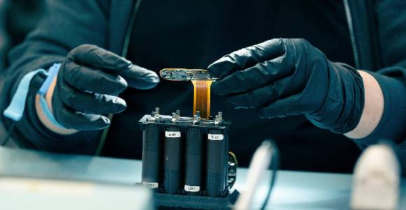
![Hands with plasticgloves holding an artifact from GomSpace]()
Research project on cybersecurity
GomSpace
“I think it's great to collaborate with universities! As a business community, we have a responsibility to give knowledge back to universities so that research becomes more concrete - more useful.”
Søren Lind Therkildsen, COO, GomSpace
-
![]()
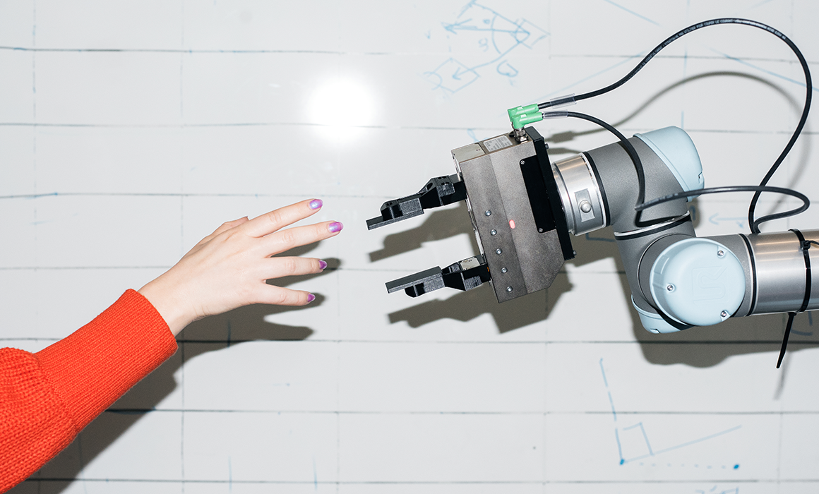
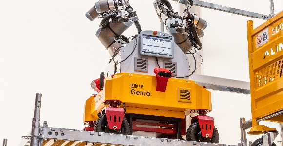
PERI
New robot technology
"The advantages far outweigh the potential challenges, so if you have the right case, I can only recommend that other companies collaborate with SDU."
Peter Rübel, Senior Business Development Manager, PERI
-
![]()
TORCH project
Open doors
“Our collaboration with SDU and the Faculty of Engineering has opened doors between museums, academia and the private sector. We’ve gained access to technologies and equipment that are crucial to our work.”
Lise Ræder Knudsen, Conservator, Conservation Centre Vejle
-
![]()
Frederiksværk Gymnasium and HF
Intervention project and supervision
"This three-year project led by SDU’s Centre for Upper Secondary School Research gave us both new insights and practical tools. It’s invaluable to bring in external experts to ensure the latest research is part of our teaching practice."
Anne Hemmingsen, Deputy Head, Frederiksværk Gymnasium and HF
-
![]()
Tietgenskolen
Accompanying research
"Our partnership with SDU’s Centre for Upper Secondary School Research gives us the data and insights we need to make the right decisions for our students. Their methods and expertise are incredibly valuable."
Jimmy Mangelsen, Principal, Tietgen Business College


Other collaboration opportunities
Write to us
Do you have any questions about collaboration?
We’re ready to help you move forward.
sdu-samarbejde@sdu.dk