Establishment of state-of-the art nanofabrication
The Zeiss ORION NanoFab Helium Ion Microscope is an advanced instrument for ultra-high resolution imaging and nanofabrication. Its operation is similar to that of a scanning electron microscope (SEM) but in contrast to SEM, the Orion microscope exploits helium, neon and gallium focused ion beams (FIB) instead of an electron beam. Because of the significantly different ion-material interaction close to the surface because of a lower beam divergence structure formation down to a few nanometers is possible.Recently we utilised focussed ion beams to
- fabricate defined individual nanostructure for nanophotonic applications
- structure surfaces without sputtering by ion beam modification of a subsurface polymer layer
- creating templates for capillarity-assisted particle assembly
Recent publications
S. Kumar, T. Leißner, S. Boroviks, S.K.H. Andersen, J. Fiutowski, H.-G. Rubahn, N.A. Mortensen, S.I. Bozhevolnyi, Efficient Coupling of Single Organic Molecules to Channel Plasmon Polaritons Supported by V-Grooves in Monocrystalline Gold, ACS Photonics. 7 (2020) 2211–2218. https://doi.org/10.1021/acsphotonics.0c00738
L. Tavares, S. Chiriaev, V. Adashkevich, R. Taboryski, H.-G. Rubahn, Height patterning of nanostructured surfaces with a focused helium ion beam: a precise and gentle non-sputtering method, Nanotechnology. 31 (2020) 145303. https://doi.org/10.1088/1361-6528/ab6679
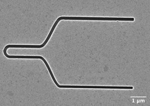 Figure 1: Plasmonic beam splitter
High resolution helium ion beam microscopy
The Zeiss ORION NanoFab Helium Ion Microscope is an advanced instrument for ultra-high resolution imaging and nanofabrication. Its operation is similar to that of a scanning electron microscope (SEM) but in contrast to SEM, the Orion microscope exploits helium, neon and gallium focused ion beams (FIB) instead of an electron beam. The imaging system of the Orion microscope offers high material contrast, large focus depth, and surface sensitivity significantly superior to conventional scanning electron microscopy. The spatial resolution is in sub-nanometer range which is close to the resolution of transmission electron microscopes. Furthermore, because effective surface charge compensation is possible, also the imaging of soft, organic materials is feasible.
Recently we utilised the instrument e.g. for imaging and analysing
- Material science: Au nanocluster growth for enhancing photocatalytic processes
- Food science: Study of diary powder
- Bio engineering: Cross-sectional imaging of spider silk
- Life-science: Structural changes of animal and human tissue caused by diseases
Recent publications
S. Veziroglu, A.-L. Obermann, M. Ullrich, M. Hussain, M. Kamp, L. Kienle, T. Leißner, H.-G. Rubahn, O. Polonskyi, T. Strunskus, J. Fiutowski, M. Es-Souni, J. Adam, F. Faupel, O.C. Aktas, Photodeposition of Au Nanoclusters for Enhanced Photocatalytic Dye Degradation over TiO 2 Thin Film, ACS Appl. Mater. Interfaces. 12 (2020) 14983–14992. https://doi.org/10.1021/acsami.9b18817
Z.J. Glover, M.J. Francis, J. Fiutowski, Q. Sun, Q. Yu, U. Andersen, J.R. Brewer, A. Cohen Simonsen, M.J. Povey, M.J. Holmes, A. Foods, Acoustic attenuation spectroscopy and helium ion microscopy study of rehydration of dairy powder, (2020). https://doi.org/10.1016/j.colsurfa.2020.124795
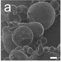 Figure 2: lactose powder
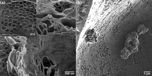
Figure 3: Mouse kidney