Boost for the development of new, advanced materials
New instrument improves analysis of high-tech nano materials
The development of new materials with advanced properties is crucial to satisfy the world's growing need for more and more efficient phones, solar cells, medicines, computers and the like. Consequently, there is also a constant need for increasingly efficient instruments for development efforts.
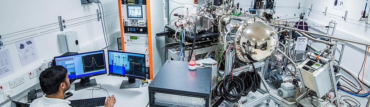
Therefore, Sven Tougaard, professor wsr in Physics at SDU, has, in collaboration with Scienta-Omicron, Henry Royce Institute, the University of Manchester and the National Physical Laboratory developed a new instrument that makes it possible to analyse a large group of such advanced materials to an unprecedented degree.
More specifically, these materials are built up of layered structures with a thickness of 100 nanometres or more. The challenge is to analyse them without destroying the structures.
Controlling the atoms
Often the many structural layers need to be heated to activate and improve their electronic, mechanical and optical properties. This can result in diffusion of atoms between the layers. This effect is undesirable, and it is extremely important to be able to determine the details of this diffusion.
Sven Tougaard has developed software and techniques that are used by hundreds of laboratories around the world to analyse the nanostructural composition of new materials.
His technique is now also used in this new instrument, which is capable of performing these analyses with unprecedented precision.
How does the new instrument work?
Sven Tougaard's method is based on the use of X-rays, which excite core electrons in the atoms. On their way out of the material, they lose energy, and it is through analysis of these energy losses that his technique can determine the position of the nanostructures in the material.
- The new instrument generates X-rays with significantly higher energy (6-7 times) than in the previous ones. My technique therefore allows us to analyse significantly deeper structures that are several hundred nanometres deep. Before, the limit was approx. 20 nanometres, he says.
Read more about Sven Tougaard's methods and software in this recently published scientific article ‘Inelastic background modelling applied to Hard X-ray Photoelectron Spectroscopy of deeply buried layers: a comparison of synchrotron and lab-based (9.25 keV) measurements’.
What are layered structures used for?
Layered nanostructures are increasingly being used for the development of materials with new advanced properties. Examples:
Within solar cell research, there is a strong focus on developing new, more efficient solar cells. In this field, research is being done into nanostructures, where multilayers with different electronic properties in a stack of layers at different depths are used to develop new solar cells that provide a higher utilisation of sunlight.
Layered structures are also used for chips in mobile phones, optical colour filters, optical mirrors, batteries and for data memory (compact discs).
Polymer layers whose outer layer has good biocompatibility properties are used in medical implants.
Meet the researcher
Sven Tougaard is Professor wsr at the Department of Physics, Chemistry and Pharmacy. He researches in the development of new techniques to determine the atomic composition and electronic properties of nanostructures.