The Zeiss Orion Helium Ion Microscope is an imaging tool with superior spatial resolution, very large depth of focus and high surface sensitivity. Combined with the ion milling capability, this allows one for 3D visualization of device failure features at micro- and nanometer length scales.
An additional advantage of the instrument is the straightforward way for compensation of the electrical charge with the electron gun which is integrated into the system. This feature provides high-resolution imaging of electrically insulating components.
The instrument is equipped with a large-volume, multi-port sample chamber that ensures easy integration of a variety of additional tools, such as ,for instances, electrical connections, optical channels, micromanipulators and accessories for correlative microscopy.
Further extension of the instrument capabilities at NanoSyd will include incorporation of a range of components and systems into the sample chamber, which will allow us for correlative microscopy in optical, Atomic-Force, and He-Ion microscopy domains.
For more information about the Zeiss Orion Helium Ion Microscope visit:
Application examples:
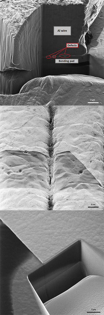
- Electronic components packaging quality analysis: Defects at the interface of an Al wire bond to a sensor chip bonding pad.
- Electronics components fabrication quality analysis: FIB etching reveales structural defects in a SiC-PE transistor. The defects manifest themselves as etch-pin-holes.
- MEMS quality analysis: Strain gauge multilayer structure in a thin film pressure sensor.
- Electrical defects localization in semiconductor devices: Passive/active voltage contrast technique.
Funded projects:
Interreg 5B program: Green PE
Interreg 5A program: PE: Region
Publications:
S. Chiriaev, N. Dam Madsen, H-G. Rubahn and S. Ma Andersen 2, “Investigation of Proton Exchange Membrane Fuel Cell Electrodes by Helium Ion Microscopy “, AIMS Materials Science, (2017) 4(6): 1289-1304
L. Tavares, V. Adashkevich, S. Chiriaev, H-G. Rubahn “FIB Nanopatterning of metal films on PMMA substrates: Non-sputtering mode”, 2nd International HeFIB conference on He and emerging Focused Ion Beams (Dresden, June 11th – 13th, 2018), p.82
S. Chiriaev, V. Adashkevich, J. Fiutowski, E. Sobolewska, J. Chevallier, H-G. Rubahn, “Metallography of thin films with focused ion beams”, 2nd International HeFIB conference on He and emerging Focused Ion Beams (Dresden, June 11th – 13th, 2018), p.38.