Organic light-emitting diodes (OLEDs) are used as energy-efficient light-emitting units e.g. for displays and lighting. Likewise, organic semiconductors can function as the light-absorbing layer in sensitive photodetector devices. Among the appealing features of organic materials for light-emitting and photodetector devices are their relative ease of processing combined with the possibility of tuning the emission or absorption spectrum via chemical synthesis of molecular building blocks with the desired characteristics. Moreover, their ^*
mechanical properties can enable the realization of mechanically flexible devices. At NanoSYD, we investigate how to realize organic thin-film materials with optimized properties and how these can be implemented into devices with high performance. More specifically, the research topics are:
- Flexible/stretchable OLEDs and electronics
- In-situ and in-operando characterization of organic thin-films and devices
- Hybrid/organic photodetector devices
- Organic nanofiber integration
Flexible/stretchable OLEDs and electronics
Bendable OLED devices can be realized by fabricating the OLED layer stack on top of a flexible substrate – typically some type of plastic film or ultrathin glass. The fabrication of a stretchable device is, however, more challenging since most of the materials used in OLED devices can only tolerate very limited stretching before breaking. At NanoSYD, we are working on the development of a new type of stretchable devices towards a stretchable OLED display. This is based on a substrate with specially designed surface corrugations. When the substrate is stretched, these corrugations flatten out but the surface itself only bends. This will enable an OLED device that can be installed on arbitrary 3-dimensional surfaces and objects. This is complemented by device simulations that provide input to experimental investigations.
In-situ and in-operando characterization of organic thin-films and devices
In order to realize organic thin-film devices with optimum performance, it is necessary to control the thin-film microstructure to obtain e.g. a certain molecular alignment and orientation. The material microstructure is formed during the thin-film deposition process and is influenced by a range of parameters related to the substrate surface, the thin-film material as well as the deposition process itself. Moreover, once the thin-film has been formed and the thin-film device has been realized, further structural and chemical changes can occur during device operation potentially degrading the performance of the device.
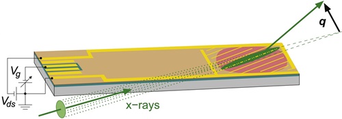
At NanoSYD, we develop and use In-situ techniques to study the thin-film formation process in order to elucidate how the various parameters influence the resulting microstructure and use this knowledge to realize devices with high performance. Moreover, In-operando techniques are developed and used to investigate microscopic changes occurring in the device materials during operation to understand their origin and mitigate their impact. This includes, for example, investigations of how the material microstructure changes in response to mechanical strain and how this affects electrical properties. These techniques include grazing-incidence X-ray diffraction as illustrated in the figure below.
Hybrid/organic photodetector devices
By combining organic semiconductors with other material classes, it is possible to realize hybrid device structures with improved properties. For example, organic semiconductors can exhibit strong optical absorption, which, combined with low price and large area processability, makes these materials useful for photodetector applications. However, their typically more moderate electrical transport properties impede the realization of fast photodetectors. This can be remedied by a hybrid device structure combining the organic semiconductor with e.g. graphene, which has superior electrical transport properties. At NanoSYD, we work on the develop and investigate photodetector devices based on both hybrid material combinations as well as pure organic semiconductor materials. In particular, we investigate how we can control the microscopic structure of the organic semiconductor material during the thin-film deposition process in order to achieve, e.g., maximum optical absorption, and how this translates into improved device performance.
Organic nanofiber device integration
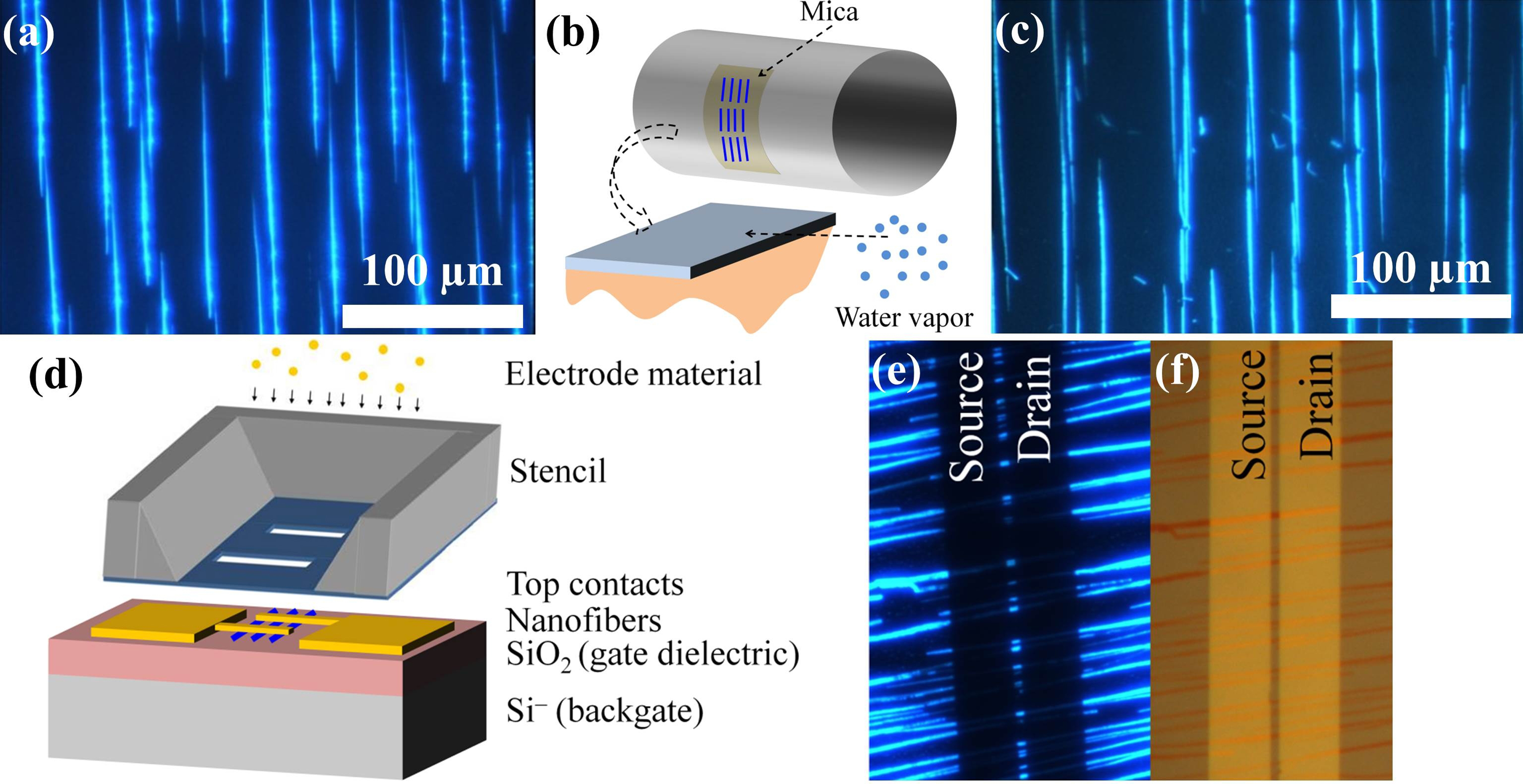
When organic films based on small molecules are used in devices, they are often deposited onto the device substrate by physical vapor deposition techniques. However, crystalline nanofibers can be formed on specific surfaces that are, however, unsuited for further processing, and special transfer techniques are therefore required for implementing such nanostructures in devices. One technique relies on the initial growth of an array of nanofibers on a muscovite mica substrate and subsequent transfer onto a device substrate via roll-printing. The process is illustrated in the figure below, on which panel (a) shows the array of nanofibers prior to transfer, panel (b) shows the principle of the roll-printing method, and panel (c) shows the nanofiber array after transfer. Afterwards, electrical contact can be established by electrode material deposition through a nanostencil as shown in panel (d), while panel (e) and (f) show the contacted nanofibers observed with a fluorescence and white-light microscope, respectively.
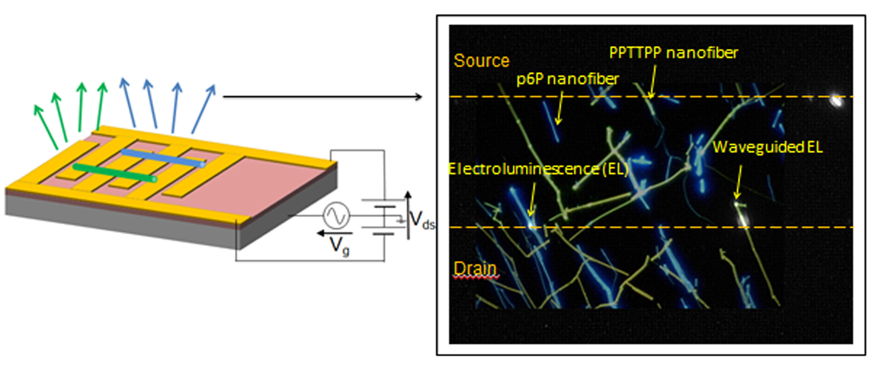
Once the nanofibers are integrated in a transistor configuration, electrical biasing with an AC voltage leads to localized light emission from the metal-organic nanofiber interfaces. This is the results of sequential injection of holes and electrons into the nanofiber and the subsequent electron-hole recombination leading to photon emission. The emission color is determined by the electronic band gap of the nanofiber material, and multicolor light- emission can therefore be achieved by integrating two different types of nanofibers with different fluorescence spectra onto the same transistor platform. The figure below shows emission from two different nanofibers as an overlay between the electrically stimulated light (grayscale) and a fluorescence microscope images from which the actual color can be seen.
NanoSYD members working within the research area
Jakob Kjelstrup-Hansen, Associate Professor
Mathias Huss-Hansen, Postdoc
Jes Linnet, PhD student
Cecilie Clausen Fynbo, PhD student
Mads Nibe Larsen, PhD student
Mark Landsperg Hempel, Master student
Tobias Schiby, Bachelor student
Simon Bruhn Hansen, Bachelor student
Thomas Mastrup Hansen, Bachelor student
Simon Valsøe Wadowski, Bachelor student
Funded projects
Development of near-infrared photodetectors for industrial applications using epitaxial growth of organic ultrathin films on 2-dimensional templates (HEXAGONAL), Independent Research Fund Denmark | Technology and Production Sciences, Research Project, 2021-2024.
The Stretchable OLED display, Innovation Fund Denmark, Industrial PhD project in collaboration with Polyteknik A/S, 2020-2023.
Methodologies for Hyperspectral Thermal Imaging, Innovation Fund Denmark, Industrial PhD project in collaboration with Newtec Engineering A/S, 2018-2021
Selected publications
Structural Effects of Electrode Proximity in Vacuum-Deposited Organic Semiconductors Studied by Microfocused X-Ray Scattering, M. K. Huss-Hansen, J. Kjelstrup-Hansen and M. Knaapila, Advanced Engineering Materials (2021) https://doi.org/10.1002/adem.202100082
Early-stage growth observations of orientation-controlled vacuum-deposited naphthyl end-capped oligothiophenes, M. K. Huss-Hansen, M. Hodas, N. Mrkyvkova, J. Hagara, P. Nadazdy, M. Sojkova, S. O. Høegh, A. Vlad, P. Pandit, E. Majkova, P. Siffalovic, F. Schreiber, J. Kjelstrup-Hansen and M. Knaapila, Physical Review Materials, 5 (2021) 053402 https://doi.org/10.1103/PhysRevMaterials.5.053402
Work function difference of naphthyl end-capped oligothiophene in different crystal alignments studied by Kelvin probe force microscopy, M. N. Larsen, M. S. Peters, R. Lemos-Silva, D. A. da Silva Filho, B. Jørgensen, O. Albrektsen and J. Kjelstrup-Hansen, Organic Electronics 89 (2021) 106060 https://doi.org/10.1016/j.orgel.2020.106060
Photo-induced and electrical degradation of organic field-effect transistors, P. P. Cielecki, T. Leißner, M. Ahmanpour, M. Madsen, H.-G. Rubahn, J. Fiutowski and J. Kjelstrup-Hansen, Organic Electronics 82 (2020) 105717 https://doi.org/10.1016/j.orgel.2020.105717
Surface-Controlled Crystal Alignment of Naphthyl End-Capped Oligothiophene on Graphene: Thin-Film Growth Studied by In Situ X-ray Diffraction, M. K. Huss-Hansen, M. Hodas, N. Mrkyvkova, J. Hagara, P. Siffalovic, B. B. E. Jensen, A. Osadnik, A. Lützen, E. Majková, F. Schreiber, L. Tavares, J. Kjelstrup-Hansen and M. Knaapila, Langmuir, 36/8 (2020) 1898 https://doi.org/10.1021/acs.langmuir.9b03467
Structural evaluation of 5,5'-bis(naphth-2-yl)-2,2'-bithiophene in organic field-effect transistors with n-octadecyltrichlorosilane coated SiO2 gate dielectric, A. Lauritsen, M. Torkkeli, O. Bikondoa, J. Linnet, L. Tavares, J. Kjelstrup-Hansen and M. Knaapila, Langmuir 34/23 (2018) 6727 https://doi.org/10.1021/acs.langmuir.8b00972
Transparent and conductive electrodes by large-scale nano-structuring of noble metal thin-films, J. Linnet, A. R. Walther, C. Wolff, O. Albrektsen, N. A. Mortensen, and J. Kjelstrup-Hansen, Optical Materials Express, 8/7 (2018) 1733 https://doi.org/10.1364/OME.8.001733
Laser-induced charge separation in organic nanofibers: A joint experimental and theoretical investigation, L. Tavares, Y. Liu, D. Behn, J. Siebels, T. Kipp, A. Mews, and J. Kjelstrup-Hansen, Organic Electronics, 53 (2018) 20 https://doi.org/10.1016/j.orgel.2017.10.032
Structural stability of naphthyl end-capped oligothiophenes in organic field-effect transistors measured by grazing-incidence X-ray diffraction in operando, M. K. Huss-Hansen, A. E. Lauritzen, O. Bikondoa, M. Torkkeli, L. Tavares, M. Knaapila and J. Kjelstrup-Hansen, Organic Electronics, 49 (2017) 375 https://doi.org/10.1016/j.orgel.2017.07.012
Enhanced photoresponsivity in organic field effect transistors by silver nanoparticles, J. Linnet, A. R. Walther, O. Albrektsen, L. Tavares, R. L. Eriksen, P. B. W. Jensen, A. Osadnik, S. Hassing, A. Lützen, and J. Kjelstrup-Hansen, Organic Electronics, 46 (2017) 270 https://doi.org/10.1016/j.orgel.2017.04.019
Multicolor nanofiber based organic light-emitting transistors, P. B. W. Jensen, J. Kjelstrup-Hansen, and H.-G. Rubahn. Organic Electronics 14 (2013) 3324 https://doi.org/10.1016/j.orgel.2013.10.001
Localized and guided electroluminescence from roll printed organic nanofibres, L. Tavares, J. Kjelstrup-Hansen and H.-G. Rubahn. Nanotechnology, 23/42 (2012) 425203 https://doi.org/10.1088/0957-4484/23/42/425203
Efficient Roll-On Transfer Technique for Well-Aligned Organic Nanofibers, L. Tavares, J. Kjelstrup-Hansen, and H.-G. Rubahn, Small 7/17 (2011) 2460 https://doi.org/10.1002/smll.201100660
AC-biased organic light-emitting field-effect transistors from naphthyl end-capped oligothiophenes, X. Liu, I. Wallmann, H. Boudinov, J. Kjelstrup-Hansen, M. Schiek, A. Lützen, and H.-G. Rubahn, Organic Electronics, 11 (2010) 1096 https://doi.org/10.1016/j.orgel.2010.03.015